- 您现在的位置:买卖IC网 > Sheet目录2000 > IDT82V3011PVG (IDT, Integrated Device Technology Inc)IC PLL WAN T1/E1/OC3 SGL 56-SSOP
Description
2
May 24, 2006
IDT82V3011
T1/E1/OC3 WAN PLL WITH SINGLE REFERENCE INPUT
DESCRIPTION
The IDT82V3011 is a T1/E1/OC3 WAN PLL with single reference
input. It contains a Digital Phase-Locked Loop (DPLL), which generates
low jitter ST-BUS and 19.44 MHz clock and framing signals that are
phase locked to an 8 kHz, 1.544 MHz, 2.048 MHz or 19.44 MHz input
reference.
The IDT82V3011 provides 9 types of clock signals (C1.5o, C3o, C6o,
C2o, C4o, C8o, C16o, C19o, C32o) and 7 types of framing signals (F0o,
F8o, F16o, F19o, F32o, RSP, TSP) for multitrunk T1/E1 and STS3/OC3
links.
The IDT82V3011 is compliant with AT&T TR62411, Telcordia GR-
1244-CORE Stratum 4 Enhanced and Stratum 4, and ETSI ETS 300
011. It meets the jitter/wander tolerance, jitter/wander transfer, intrinsic
jitter/wander, frequency accuracy, capture range, phase change slope,
holdover frequency accuracy and MTIE (Maximum Time Interval Error)
requirements for these specifications.
The IDT82V3011 can be used in synchronization and timing control
for T1, E1 and OC3 systems, or used as ST-BUS clock and frame pulse
source. It also can be used in access switch, access routers, ATM edge
switches, wireless base station controllers, or IADs (Integrated Access
Devices), PBXs, line cards and SONET/SDH equipments.
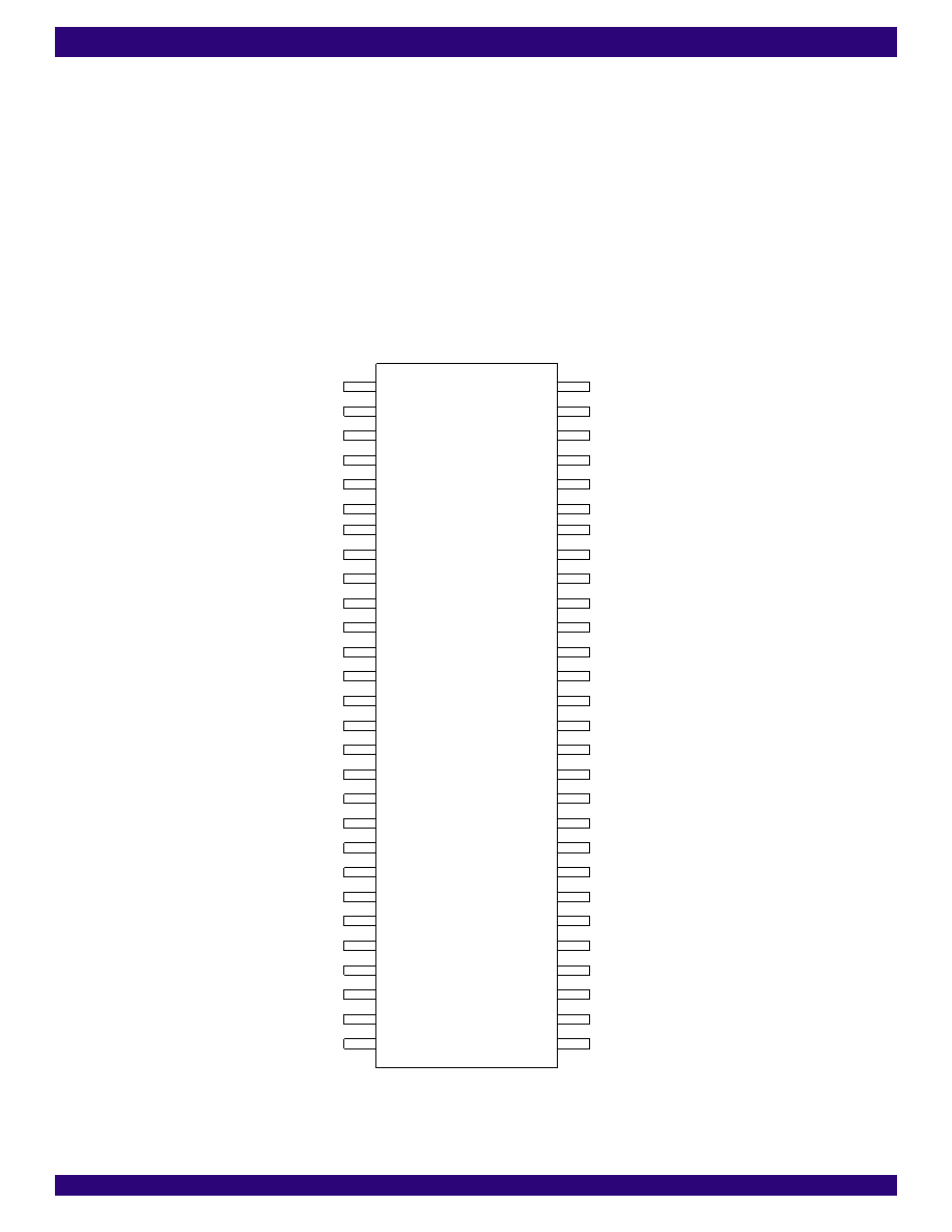
PIN CONFIGURATION
Figure - 1 IDT82V3011 SSOP56 Package Pin Assignment
IDT82V3011
14
15
16
17
18
19
20
21
22
23
24
RST
MON_out
IC
Fref
F19o
OSCi
F8o
C1.5o
LOCK
C2o
C4o
FLOCK
F_sel1
F_sel0
C3o
C8o
C16o
C32o
F0o
F16o
1
2
3
4
5
6
7
8
9
10
11
12
13
56
55
54
RSP
TSP
C6o
VDDD
TDI
TMS
TRST
TDO
TCK
IC0
HOLDOVER
FREERUN
NORMAL
TIE_en
VDDD
VSS
C19o
MODE_sel0
MODE_sel1
TCLR
IC
25
26
27
53
52
51
50
49
48
47
46
45
44
43
42
41
40
39
38
37
36
35
34
33
32
31
30
28
29
VDDD
VSS
VDDA
VSS
F32o
VSS
VDDA
C2/C1.5
IC2
IC
C19NEG
C19POS
IC
发布紧急采购,3分钟左右您将得到回复。
相关PDF资料
IDT82V3012PVG8
IC PLL WAN T1/E1/OC3 DUAL 56SSOP
IDT82V3155PVG
IC PLL WAN T1/E1/OC3 DUAL 56SSOP
IDT82V3202NLG
IC PLL WAN EBU SGL 68-VFQFPN
IDT82V3255TFG
IC PLL WAN SMC STRATUM 3 64-TQFP
IDT82V3280APFG
IC PLL WAN SE STRATUM 2 100TQFP
IDT82V3285AEQG
IC PLL WAN SE STRATUM 100TQFP
IDT82V3285EQG
IC PLL WAN SE STRATUM 100TQFP
IDT82V3288BCG
IC PLL WAN 3E STRATUM 2 208CABGA
相关代理商/技术参数
IDT82V3011PVG8
功能描述:IC PLL WAN T1/E1/OC3 SGL 56-SSOP RoHS:是 类别:集成电路 (IC) >> 时钟/计时 - 专用 系列:- 标准包装:1,500 系列:- 类型:时钟缓冲器/驱动器 PLL:是 主要目的:- 输入:- 输出:- 电路数:- 比率 - 输入:输出:- 差分 - 输入:输出:- 频率 - 最大:- 电源电压:3.3V 工作温度:0°C ~ 70°C 安装类型:表面贴装 封装/外壳:28-SSOP(0.209",5.30mm 宽) 供应商设备封装:28-SSOP 包装:带卷 (TR) 其它名称:93786AFT
IDT82V3012
制造商:IDT 制造商全称:Integrated Device Technology 功能描述:T1/E1/OC3 WAN PLL WITH DUAL REFERENCE INPUTS
IDT82V3012PV
制造商:Integrated Device Technology Inc 功能描述:
IDT82V3012PVG
功能描述:IC PLL WAN T1/E1/OC3 DUAL 56SSOP RoHS:是 类别:集成电路 (IC) >> 时钟/计时 - 专用 系列:- 标准包装:1 系列:- 类型:时钟/频率发生器,多路复用器 PLL:是 主要目的:存储器,RDRAM 输入:晶体 输出:LVCMOS 电路数:1 比率 - 输入:输出:1:2 差分 - 输入:输出:无/是 频率 - 最大:400MHz 电源电压:3 V ~ 3.6 V 工作温度:0°C ~ 85°C 安装类型:表面贴装 封装/外壳:16-TSSOP(0.173",4.40mm 宽) 供应商设备封装:16-TSSOP 包装:Digi-Reel® 其它名称:296-6719-6
IDT82V3012PVG8
功能描述:IC PLL WAN T1/E1/OC3 DUAL 56SSOP RoHS:是 类别:集成电路 (IC) >> 时钟/计时 - 专用 系列:- 标准包装:1,500 系列:- 类型:时钟缓冲器/驱动器 PLL:是 主要目的:- 输入:- 输出:- 电路数:- 比率 - 输入:输出:- 差分 - 输入:输出:- 频率 - 最大:- 电源电压:3.3V 工作温度:0°C ~ 70°C 安装类型:表面贴装 封装/外壳:28-SSOP(0.209",5.30mm 宽) 供应商设备封装:28-SSOP 包装:带卷 (TR) 其它名称:93786AFT
IDT82V3155
制造商:IDT 制造商全称:Integrated Device Technology 功能描述:ENHANCED T1/E1/OC3 WAN PLL WITH DUAL REFERENCE INPUTS
IDT82V3155PV
制造商:IDT 制造商全称:Integrated Device Technology 功能描述:ENHANCED T1/E1/OC3 WAN PLL WITH DUAL REFERENCE INPUTS
IDT82V3155PVG
功能描述:IC PLL WAN T1/E1/OC3 DUAL 56SSOP RoHS:是 类别:集成电路 (IC) >> 时钟/计时 - 专用 系列:- 标准包装:1,500 系列:- 类型:时钟缓冲器/驱动器 PLL:是 主要目的:- 输入:- 输出:- 电路数:- 比率 - 输入:输出:- 差分 - 输入:输出:- 频率 - 最大:- 电源电压:3.3V 工作温度:0°C ~ 70°C 安装类型:表面贴装 封装/外壳:28-SSOP(0.209",5.30mm 宽) 供应商设备封装:28-SSOP 包装:带卷 (TR) 其它名称:93786AFT